Week 6: Electronics Design
Assignment:
- Redraw the echo hello-world board, add (at least) a button and LED (with current-limiting resistor), check the design rules, make it (if you have time this week, test it).
- Optional: simulate its operation. Measure its operation
For this assignment the goal is learn how to work with Eagle to be able to redesign the board and adding a LED and button to the components it already have.
Machines:
- Trotec Speedy 100
- Soldering Heat Gun
Software:
Materials:
- Spray Paint
- Removable adhesive liner paper
- Copper Board
- Ferric Perchloride
- Solder Paste
- Tweezers
- Antistatic table
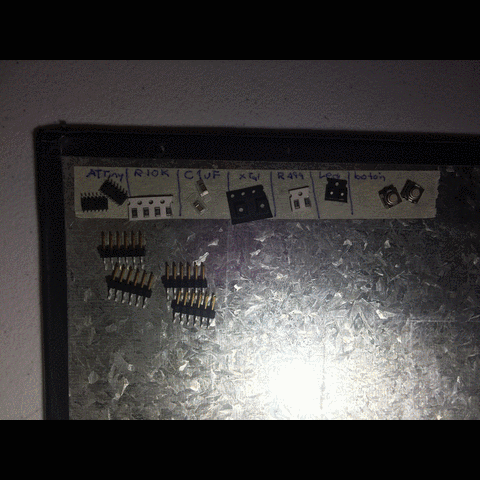
Electronic Components:
- 1x 6-pin programing header
- 1x 6-pin line connector
- 1x Microcontroller ATTiny 44
- 1x FTDI header
- 1x Crystal Resonator 20 MHz
- 2x Resitor 10K
- 1x Ceramic capasitor 1uF
- 1x LED red
- 1x Button 0.05A 24V
- 1x Resitor 499 Ohm
WORKING WITH EAGLE
I decided to work on Eagle because I felt comfortable with its interface and performance. Eagle is a software to design PBC boards, and this time we learn how to use it.
First step was download Eagle and install it in the computer, in my case I downloaded Mac version.
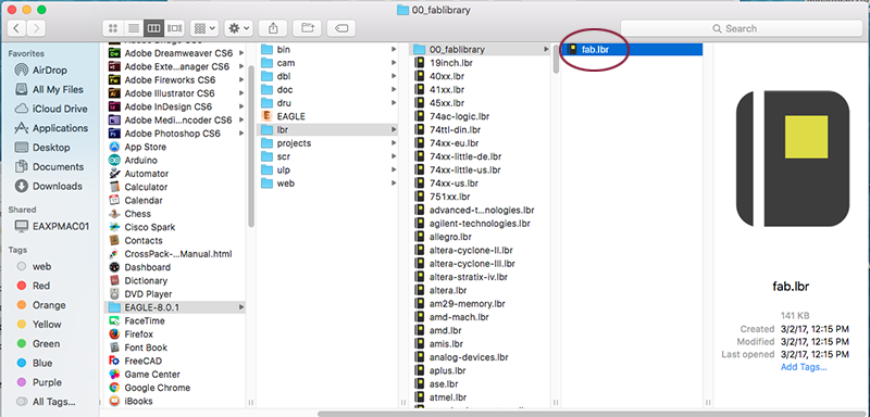
Once the software was installed in the computer, I donwnloaded the Fab Academy Eagle library fab.lib which makes easier to find the necessary components to design the boards along the process. This file should be in the "lib" folder inside Eagle folder in Applications.
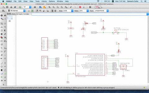
Eagle works with two different windows, schematic and board. Schematic is a drawing representing the circuit using symbols for each electronic component used, and board shows how the electrical components and traces will be laid out on the board. Both windows depend one of the other and you should work with them to design a PCB.
In Eagle is optional to work with command line or graphical iconts tool bar, in my case I almos just use the icons because I'm used to work that way, but some commands were easier in command line.
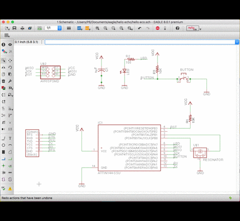
As I don't have any background knoledge in electronics, my firs step was use Neil's schematic as guide and I did everything again. At the beginning I started to draw lines to connect components, but sooner it was a mess and I found in the tutorial that it was possible to name the wires an connect them that way instead of draw lines for all the schematic page, it was lots easy!
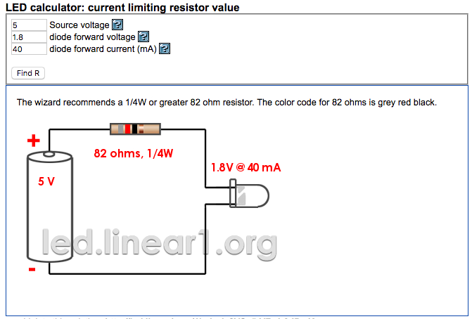
Next step was add a LED and button, to avoiding the possibility of burn components, the LED should has a resistor to protect its performance, so I use a LED calculator to find the right resistor using the information in the component data sheet that says :
- Source Voltage: 5V
- Forward Voltage: 1.8 if 20 mA
- Forward Current: 40 mA
So the calculator said that I should need an 82 Ohm resitor, so using one 100 Ohm is the nearest and sohould be OK, but I decided to use a 499 Ohm resistor because is the one I have.
Once I finished to connect and place all the components in schematic window, next step was go to board window and locate all the components once and again, using Neils board and trying to do it as simmilar as possible adding the LED and the button, and I finish the board succesfully.
I exported the board layer 1 in PNG format and monochromatic, then import the PNG fil to Illustrator CS6 to redraw the pads and lines to engrave in the Trotec Speddy 100 as I did in Week 4 asignment, because I don't have a milling machine to mill the board. Here is the result:
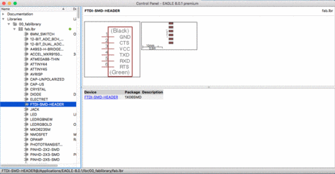
When I finished my board, I show my work to the instructor to see if everything was OK and it was matter of time to figure out that, by a mistake in the components list, we have the wrong 6 pin connector, so we are not able to use it because is too tiny and we don't have cables to connect it, so the solution to this problem was create a new one in the fab library using another FTDI 6 in line pins insted.
To create a new component in the library I followed the next steps:
- In Control Panel window open Fab library and select the component name FTDI-SMD-HEADER.
- Create a new library and copy the component by dregging it.
- Right click on the component name and select “open in library”, then the component window will appear and click on the “symbol” icon in the tool bar to edit the package contents.
- Change the connector pins names and save before close.
- Now a new component is available in the library and ready to use.
Now I changed the component in schematic and in board windows, and start to draw the lines again. At first it was a little difficult because the board should look completely different to the first one and the lines should be drawn in different ways, but I finally could design my board.
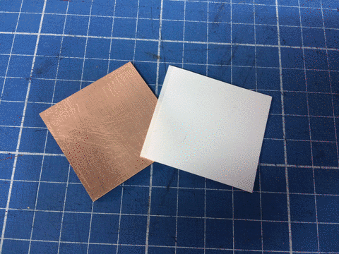
As same as the first one, I export to PNG and place it in Illustrator to draw all the pads and lines. First I try to do the same process of week 4 assignment: paint the copper board, engrave and clean, but this time it was lots of difficult because the lines are thiner than the FabISP and it didn’t work at all, so I decided to do something different.
In week 4 I tried unsuccessfully to cut a stencil to paint over it, but now I have some removable adhesive liner paper and it worked! I avoid the process to clean the board! The adhesive liner paperI used is a Xerox product used for laser digital printing.
- Just apply the ahesive liner paper over the clean copper board and laser cut the pads and lines.
- Remove the vinyl pieces of pads and lines and apply a thin coat of black spray painting, because where the painting is, are the copper pieces we want to preserve, and the other ones will dissolve in the etching process.
Here is the result:
Next step is etch the board in ferric per chloride to get the copper board finished, using the same process I used in week 4.
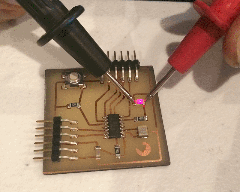
To soldering the components in the board I apply again soldering paste using a stencil and placed the components in their respective pads. Then with a hot soldering gun I heat the pads until melt the soldering paste, to know when to stop apply hot air, is when the soldering pads tuns silver and shiny.
This is how my hello-world PCB board looks after soldering.
Then, with the help of a tester device, I test the LED and button and thankfully they work well.
This assigment was sponsored by: